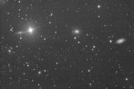
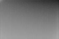
Vertical banding in stacked CCD images

I get vertical banding in my stacked
images, similar but not identical to the issue Adam resolved by adding a pedestal
to narrow band data, and mine occurs with all filters. The camera is an SBIG
STXL 11002.

I am in contact with SBIG and they
feel that it is a processing issue. I noted that I have had the camera for some
5 years now and it has only been doing this in the last 6 months. I sort of
work around it by super smoothing with RC’s NoiseXterminator but it still shows
of course. It is much worse in the binned data.

I have tried the following unsuccessfully:

1)     Adding a pedestal

2)     Changing the power supply

3)     Bypassing a data hub

4)     Using a master dark in Cosmetic Correction along with my
usual auto detect

5)     Using linear defects correction in WBPP

6)     Skipping the flats to remove the flat panel from the
loop

7)     Skipping Local Normalization in WBPP to remove it from
the loop

Nothing seems to work. I believe what
I see on the stacked image is the result of subtle regular banding in the chip
that, once dithered, shows up when stacked.

Any advice would be appreciated. Raw
data is available here:

https://wetransfer.com/downloads/bcda19f6ffb9845bb0ecdd8eb2cb558820230419194156/422bf48d07f6fd51f6890bd2b5a2311e20230419194156/66c26b?trk=TRN_TDL_01&utm_campaign=TRN_TDL_01&utm_medium=email&utm_source=sendgrid

Mark


thumbnail_masterLight_BIN-2_2004x1336_EXPOSURE-300.00s_FILTER-Red_mono.jpg
640 x 426 - 70K
masterBias_BIN-2_2004x1336.jpg
2004 x 1336 - 324K
masterDark_BIN-2_2004x1336_EXPOSURE-300.00s.jpg
2004 x 1336 - 634K
masterFlat_BIN-2_2004x1336_FILTER-Blue_mono_MERIDIAN-E.jpg
2004 x 1336 - 31K

Comments

  • This isn't vertical banding... but a normal aging effect for a real CCD sensor of this type. (The 16803 did the same thing). I think I still have the videos on it somewhere- but you basically need to dither your data and when processing use a defect map. Using a defect list in Cosmetic Correction can do it..but I prefer to make the actual image. 

    It is an old video.. but the defect map part might be useful:

    -the Blockhead
  • Many thx. I will give it a try.
  • I carefully modelled the bright columns the best I could, but it did not work. I have attached the defect map.

    I did notice that what shows in the image is more the dark bands rather than the bright ones. I will try to model them instead and try again.

    Weird thing is that they seem to appear +-15 pixels apart in a very regular pattern which surprises me a bit. It's not random.

    DefectMap_brightColumns.jpg
    2004 x 1336 - 695K
  • The fainter ones really should not be an issue. The black ones are the ones to concentrate on. 
    The key to getting a clean image is dithering by large values (randomly 5 or more pixels) and taking many images (20+). Rejection alone really should do a majority of the work, but applying a cosmetic adjustment with a defect map should help. 

    I have not done it in a while...so if you have a set of raw luminance data with calibration files..I can perhaps make a section. I thought I had one where I make the defect map.. but I do not obviously see one now.

    -the Blockhead
  • All the raw data is available thru the link in my original post if necessary.

    I did find your video on creating the defect map and that’s the technique I used to create mine. You have quite a library now, congrats. The search tool is a must and worked well.

    I had dithered up to 3 pixels. Given the pattern is +-15 pixels trough to trough, I will increase that to 8 in future acquisitions. I agree that greater dithering is probably the best fix, as the effect is quite subtle and I did not see many really black ones.

    I am gradually moving over to CMOS but I have several CCDs that have served me well and will be costly to replace.

    Thanks again for your help.
Sign In or Register to comment.